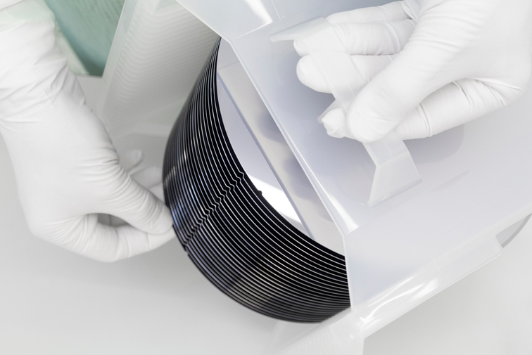
Germanium (Ge) Wafers

Overview
Germanium (Ge) wafers are high-purity semiconductor wafers known for their excellent electron mobility and infrared optical properties. Germanium’s unique characteristics make it a critical material in advanced electronics, high-performance photodetectors, and solar cells. With a direct bandgap and a relatively high atomic number, germanium is also an essential component in optoelectronic devices and infrared optical systems. Its widespread use in multijunction solar cells, infrared optics, and high-frequency electronics underscores its versatility and importance in cutting-edge technologies.
Product Features
High Efficiency Light Emission
InGaP wafers are known for their high-efficiency light emission, making them ideal for LEDs, laser diodes, and optoelectronic devices.
High-Frequency Performance
These wafers are commonly used in radio frequency (RF) and microwave devices due to their ability to function effectively at high frequencies, including in mobile communication systems and satellite technologies.
Solar Cell Efficiency
InGaP wafers are often used in the top layers of multijunction solar cells, providing excellent efficiency in converting sunlight to electricity, especially in space and high-performance terrestrial solar applications.
Thermal Stability
InGaP’s ability to maintain performance under high temperatures makes it suitable for applications that require stability in extreme environments.
- Wafer Sizes: Available in diameters of 2-inch, 3-inch, 4-inch, and 6-inch.
- Thickness: Customizable thickness options based on specific application needs, typically ranging from 250 µm to 700 µm.
- Resistivity: Available in both high-resistivity and low-resistivity grades, depending on the electronic application.
- Surface Finish: Can be supplied with polished or unpolished surfaces, depending on the optical or electronic use case.
- Doping: N-type or P-type doping is available to customize the electrical properties of the wafer for specific electronic applications.
- Crystallographic Orientation: Available in standard orientations, including (100), (111), and (110), to meet different application requirements.
- Infrared Optics: Germanium wafers are widely used in infrared optical systems, including thermal imaging, night vision, and infrared spectrometry due to their high transparency in the infrared spectrum.
- High-Efficiency Solar Cells: These wafers are a key component in multijunction solar cells, particularly in space applications, where efficiency and weight are critical.
- High-Speed Electronics: Germanium wafers are used in the fabrication of high-frequency transistors, integrated circuits, and other high-speed electronics, where their superior electron mobility provides a significant performance advantage.
- Photodetectors and Sensors: Germanium’s properties are leveraged in photodetectors and optical sensors that require sensitivity to infrared light, including environmental monitoring and telecommunications applications.
