
Sapphire Wafers
Overview
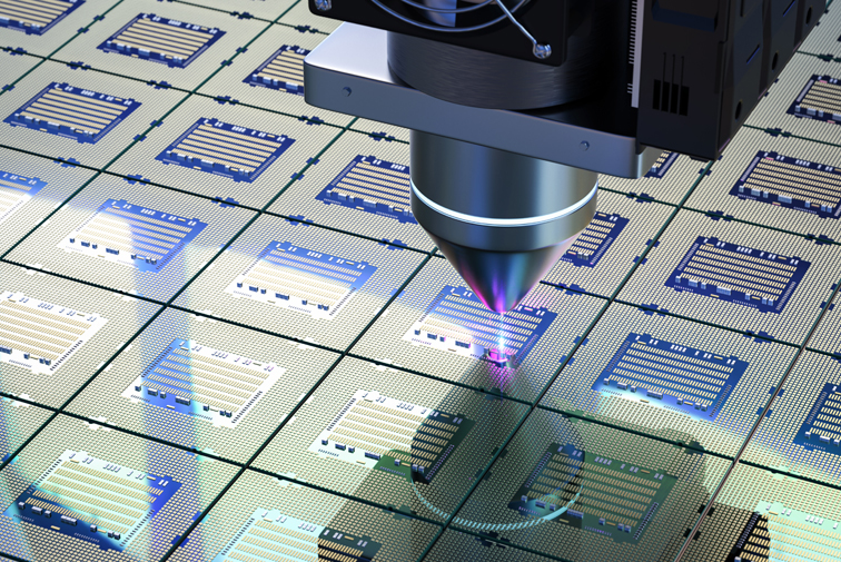
Sapphire wafers are widely recognized for their exceptional hardness, high thermal stability, and excellent optical transparency, making them indispensable in a variety of high-performance applications. As a single-crystal form of aluminum oxide (Al₂O₃), sapphire wafers are used extensively as substrates for gallium nitride (GaN) devices, LEDs, and semiconductor applications. Due to their optical clarity in the ultraviolet (UV), visible, and infrared (IR) ranges, sapphire wafers also play a critical role in advanced optics, sensors, and photonics. Their combination of mechanical strength and thermal resistance makes them ideal for use in harsh environments where durability is crucial.
Product Features
High Hardness and Durability
Sapphire is second only to diamond in hardness, providing extreme resistance to scratches, wear, and mechanical damage, making sapphire wafers suitable for rugged environments.
Optical Transparency
Sapphire’s transparency across a broad wavelength spectrum (UV to IR) makes it an ideal material for optical windows, lenses, and photonics applications where clarity and precision are essential.
Thermal Stability
Sapphire wafers can withstand extremely high temperatures, maintaining stability and performance in high-power electronic applications and other environments exposed to heat and radiation.
Electrical Insulation
With excellent insulating properties, sapphire is widely used as a substrate in semiconductor devices, particularly in gallium nitride (GaN) and silicon-on-sapphire (SOS) technologies.
- Wafer Sizes: Available in a range of diameters, typically from 2-inch to 6-inch, with custom sizes available to meet specific application requirements.
- Thickness: Standard thicknesses range from 250 µm to 700 µm, customizable to specific project needs.
- Surface Finish: Can be provided with polished, semi-polished, or unpolished surfaces, depending on the optical or electronic use.
- Crystal Orientation: Standard orientations include C-plane (0001), A-plane (11-20), and R-plane (1-102), selected based on the intended device application.
- Optical Properties: Transparency in the UV, visible, and IR ranges with high transmittance and low birefringence, critical for optical and photonic applications.
- LEDs and Optoelectronics: Sapphire wafers are the primary substrate for GaN-based LEDs and laser diodes, which are used in lighting, displays, and optical communication devices.
- Optics and Photonics: Sapphire’s clarity and durability make it an ideal material for optical components like windows, lenses, and prisms, particularly in high-precision instruments and harsh environments.
- Semiconductor Substrates: Sapphire wafers are used in GaN devices, silicon-on-sapphire (SOS) integrated circuits, and other high-performance semiconductor applications that require superior thermal and electrical performance.
- Sensors and Medical Devices: Due to their biocompatibility and resistance to wear, sapphire wafers are often used in sensors, watch crystals, and medical implants.
- High-Temperature Applications: The thermal and mechanical properties of sapphire wafers make them well-suited for use in high-temperature, high-stress environments such as aerospace and defense.